In the Eigler group, we focus on the…
Fabrication of transistor-type devices to determine the charge transport properties of 2D materials and assemblies.
Fabrication of Devices and Measurement of Transport Properties
Atomically thin graphene-based materials suffer significant mobility degradation due to charged impurities and photo scattering induced by silicon oxide-covered silicon (SiO2/Si) substrates. However, within devices those properties can be determined. Up to now, the influence of chemical modification on the transport properties are difficult to predict. Control of doping, tuning of resistance and the interaction with environmental molecules can be evaluated. Therefore, we set-up the technology to make devices from single flakes of 2D materials in general and chemically prepared flakes of graphene in particular.
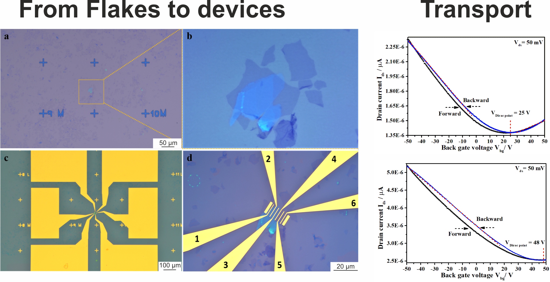
Device structures can be seen in the figure from flakes, or overlapping flakes to the measureable device. Typical I-V curves are shown on the right side.
In the future we will focus on the fabrication of 2D architectures to further control interactions with molecules to understand sensing applications.